“This blog describes how to emulate UART using Simple GPIO, Timer and external Interrupt”
Emulated UART requires in the application where UART
peripheral available on the controller is not free to communicate with other
device through UART communication.
UART will be emulated through simple GPIO pins, External
Interrupt ant Timer peripherals. GPIO pins will be used as Transmitter and
receiver pin. Timer peripheral used for
generating timing event according to UART communication baud rate.
Figure below show the simple block diagram of UART emulation
through Microcontroller.
In this Simple GPIO pins will be as
Tx and Rx pins. Data will be transmitted by SET and RSEST of transmitter pin at
specific time interval on timer overflow event. Data transmission is handled by
Transmitter module. MCU detect receiving data through external Interrupt event
and reading Rx pin status. Receiving function is handled by Receiver module.
Data generator module handles all data formatting and communication status flag
monitoring.
Transmitter Working
The principle behind simulating UART transmitter is
configure transmitter pin in output mode and changing signal level between GND
and VDD at timer overflow interrupt
event according to data to be transmitted. In this transmitter overflow period
will be half of the bit period that depends on the baud rate.
For example if our baud rate is 9600 bps then bit period
will be around 104 usec and half of the bit period will be 52 usec. Timer will
be configured to generate interrupt after every 52 usec if timer is enabled.
At idle state timer will be disabled and Tx pin output
status will be High (VDD). When there will be data transmission request CPU Low
(Start Bit) the Tx Pin and Enable Timer module configured to half bit period.
In timer interrupt there will be Counter
that will be increment by one after every interrupt event. After Start Bit
transmission CPU will monitors the monitor the Counter value. At each even Counter value CPU change the status of
Tx pin according to data to be transmitted. When complete 8 or 9 bit data is
transmitted CPU pulls the Tx pin to VDD (End bit) and after successful
transmission of End Bit clear the Counter Value and disable the Timer
module.
For example we have to transmit 8-bit data 0x55. As shown in
figure above 8 bit data to be transmitted is 0x55. So the complete frame
structure will be:
Figurer below show the Timing diagram and Tx Pin status
according to data 0x55:
As shown in figure
above Initially Tx pin will be in idle state (pulled VDD) and TC (Transmission
Complete) flag will be high. When there will request for data transmission CPU
pulls the transmitter Pin to ground, TC flag and enable Timer Module configured
to half but period. In Timer Overflow interrupt routine CPU increment the
Counter Flag by one each time. On the even value of Counter CPU change the Tx
Pin status according to data. After complete data transmission CPU disable the
timer and clear the Counter value. After
complete data transmission CPU set the TC (Transmission Complete) flag to 1.
Receiver Working
Principle behind
simulating UART receiver is firstly detect the start bit using external
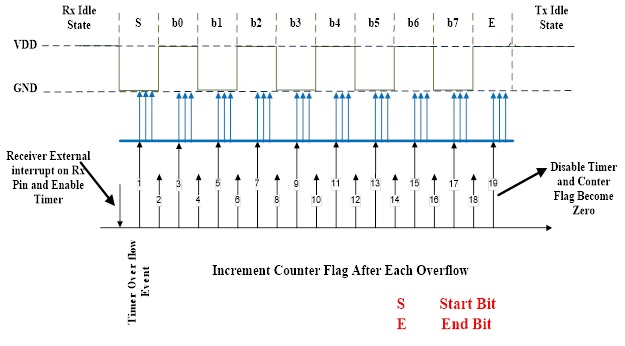
interrupt on Rx pin and then taking 3 sample of the Rx signal at ODD value of Counter. If three samples are same then
CPU consider it a valid data bit and if samples are different then CPU SET the FE (Framing error) Flag configure
Receiver Module to Idle state. After successfully start bit detection CPU clear
the RC (Reception complete) Flag.
And after complete byte reception (detection of End Bit) CPU RC flag.
As shown in figure
above receiving procedure starts after detecting external interrupt on Rx pin.
Rx pin is configured to external interrupt on falling low event. When start bit
(0) of data occurs on the Rx pin CPU get interrupted. After interrupt event CPU
Reset the RC flag, disable the
External interrupt on Rx pin and enable timer module configured to half data
bit rate overflow time period. In Timer Overflow interrupt routine CPU
increment the Counter Flag by one each time. On the ODD value of Counter CPU poll the Rx Pin status.
If all three samples are same CPU consider it
a valid data bit. CPU ignores the even counter values. In the same way CPU
detects all data bits and when CPU receives completed data byte it will disable
the timer, clear Counter, set RC flag and enable External interrupt
to receive next byte.
If all three samples
are not same CPU consider it as Corrupted data and set FE flag. After this CPU
configure receiver module to idle state.


No comments:
Post a Comment